
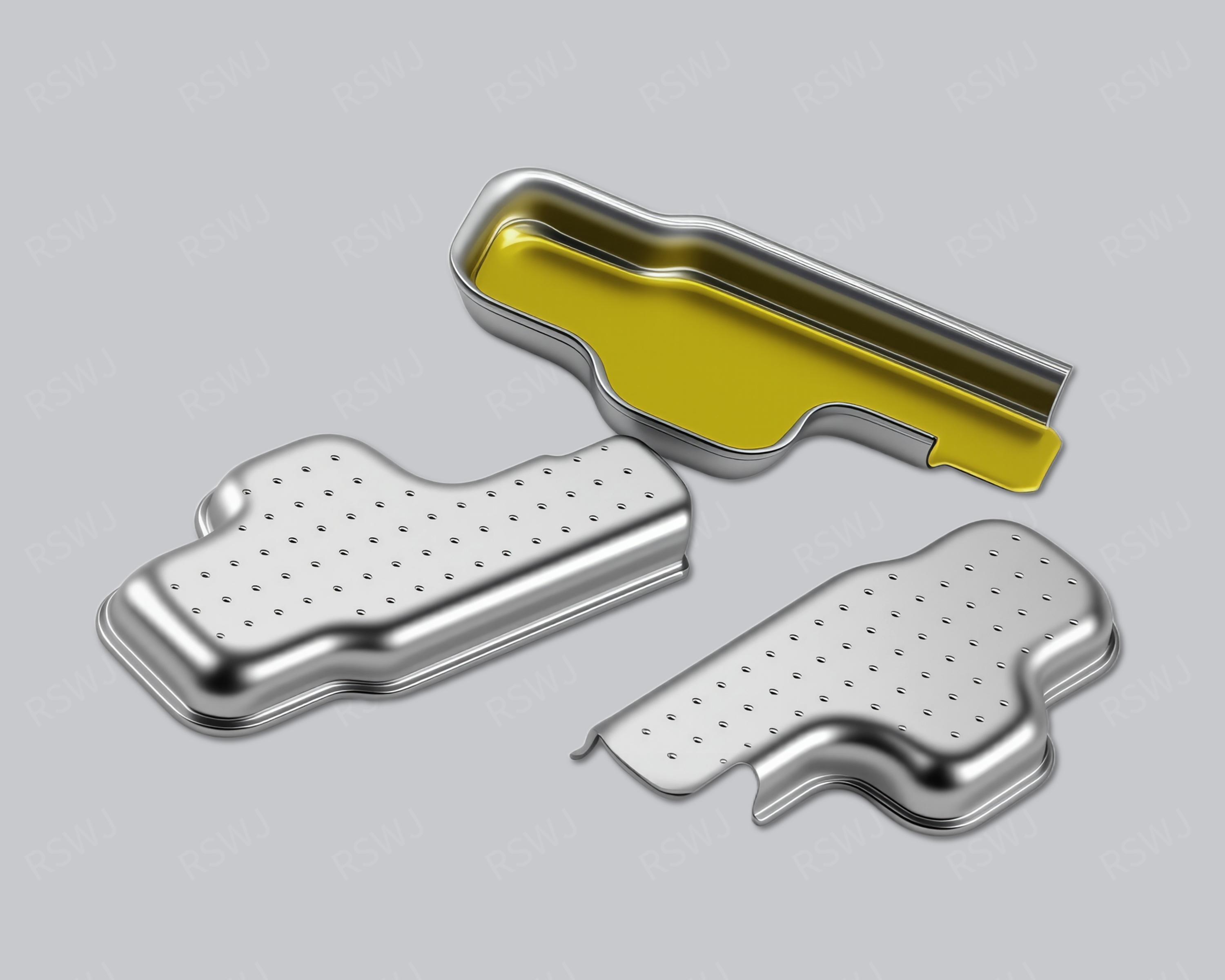
Reference photograph. Material, dimensions and mating requirements are defined in the agreed project drawings.
Resolve the circuit label before specifying the cover
A BT circuit shield retains the project label while the covered function and interface are defined from the layout.
| Design focus | Project-defined BT circuit, device locations, external interfaces and reserved regions |
|---|---|
| Project task | Resolve the circuit label before specifying the cover |
| Custom inputs | Current drawings, mating parts, material and final surface, quantity and acceptance requirements. |
Resolve the circuit label before specifying the cover
BT is a project label. Define its circuit function on the layout before specifying coverage; it does not automatically identify Bluetooth or another particular function.
Define the meaning of BT in the project and annotate the corresponding devices before selecting a coverage boundary. If it names a wireless region, antenna and feedline arrangements become relevant; if it is another project abbreviation, use that function’s actual interfaces instead. This clarification changes the design inputs, not merely the page title. Keep the confirmed term in sample and drawing records so supplier and integration teams discuss the same region.
Engineering considerations for this project
Turn the BT label into a usable circuit definition
A BT-labelled shielding request needs an unambiguous description of the covered function before the structure is selected. Identify the devices represented by the label on the actual layout and state the interfaces linking that region with the rest of the board. The abbreviation can remain as the customer's part or region identifier, but it should accompany information that another team can use. This makes the design review practical without assigning a wireless, processor or other meaning from the letters alone. The cover geometry can then follow the defined circuit and assembly relationships. Show the agreed region description beside the part identifier in review files so the physical task remains clear during subsequent handoffs.
The region view should mark its fixed attachment references and functional exclusions. Once the task is clear, identify what needs coverage, what must remain accessible and what connecting operation constrains the walls or openings. A project name does not explain those choices. If the initial information is only a sketch or physical reference, record which relationships are confirmed and which still need definition. The next drawing can close those open items progressively, giving the quotation and sample proposal a controlled scope instead of asking them to compensate for an unresolved circuit-area description.
Choose geometry from confirmed interfaces rather than assumptions
A defined interface can be reviewed through the same practical questions regardless of its internal abbreviation. Show the corresponding PCB or base, component envelope and neighboring structures that restrict the part. Include the motion needed for installation or connection as well as the seated condition. The engineer can compare a fixed body, upper cover or another arrangement through those inputs. If the circuit definition changes, revisit the boundary and access need directly. This keeps the structural choice tied to confirmed relationships and avoids retaining a convenient outline that was developed around an earlier interpretation of the label.
Material and final surface requirements should follow the part's actual attachment, mating and project conditions. State them separately from the circuit identifier and locate the functional regions on the drawing. If an option remains open, identify the question it is intended to resolve and the requirements that must stay fixed. A sample can then assess a specific formed feature or installed interface using the corresponding counterpart. This approach allows a BT project to move forward even where the customer uses internal terminology, provided the manufacturing brief describes the physical and functional requirements clearly.
Keep the clarified terminology in the approval record
The sample and drawing records should use the agreed circuit description together with the customer's BT identifier. Identify the board or mating revision and the installation condition used to check the part. Customer evaluation follows the confirmed function and project objective, with the relevant operating configuration retained. This prevents different teams from attaching different meanings to a sample result or selecting unrelated assessment conditions. A geometric concern can be located through the drawing, while an application observation remains connected to the circuit definition that gave the shielding boundary its purpose.
If the customer later revises the region or the meaning of the identifier, compare the changed function and interfaces with the approved brief. A renamed region may leave the geometry unchanged, while a retained label can accompany a substantive layout change. State which situation applies and select the recheck from the physical consequence. This makes repeat purchasing and another custom proposal understandable across teams. The useful approval basis is the clarified circuit and installed part arrangement, not an assumed expansion of BT or a claim that one photographed cover is suitable for every task using those letters.
Boundary, clearance and mating design
Locate the designated devices and signal interfaces on the board. Once the function is clear, define the coverage, reserved regions and adjacent electronic partitions.
Translate the application into an actual circuit region. Mark the devices, interfaces and surrounding functions involved in the project concern. The equipment name can help organize discussion, but it does not provide hidden dimensions, compatibility or operating performance. Identify what must remain outside the metal boundary, such as a functional antenna, optical region or connection operation. The perimeter then follows a defined electronic and mechanical task rather than an arbitrary rectangle around the board.
Material and final surface definition
Select the material and final surface through forming, attachment, contact and the customer environment. The application label does not determine an alloy or coating for the reference. Specify grade, condition and thickness where required, with the final treatment separate. A working cover edge and a board joining region may need different checks. If a material alternative is evaluated, keep its changed conditions clear instead of treating it as an interchangeable color or marketing designation.
Forming and the installation sequence
Review installation, connecting parts and required access from the actual assembly. The abbreviation does not establish the attachment method or finished cover dimensions.
Use the real mounting references and component envelopes to establish fit. Review the path used to place the shield, connect interfaces and fit the surrounding housing. The final position can clear a connector while the required insertion motion remains blocked. Mark intentional contacts separately from required gaps. When another part loads the roof, check the installed state rather than using an unloaded cover height as the full clearance decision.
Resolve the label before choosing the evaluation method
Once the BT circuit function is identified, compare coverage and access through that function’s actual interfaces. Do not assign radio, antenna or processor assumptions from an unresolved abbreviation. Mark the covered devices and connections on the layout and use an unambiguous region name in the drawing package. This first clarification can change the required boundary and the sample plan, making it a substantive engineering decision rather than an editorial naming preference.
Part inspection and application evaluation
Tie the test plan to the confirmed function and operating states. Sample records should use an unambiguous circuit-area name so results remain understandable across teams.
A drawing package for this custom part
| Input | What makes it usable |
|---|---|
| Coverage & interfaces | Project-defined BT circuit, device locations, external interfaces and reserved regions. Mark their relationship with the actual circuit or mating layout; identify fixed references and permitted changes. |
| Final part & datums | A dimensioned finished-part drawing and available 3D information. Identify functional dimensions, the installed condition and the measurement references used to accept them. |
| Material & surface | The specified grade, condition, thickness and final treatment. Show contact, joining and insulated regions separately; identify any alternative that needs evaluation. |
| Assembly & acceptance | Corresponding mating revisions and the installation or access sequence. Distinguish part inspection, matched fit and customer system checks with their agreed conditions. |
Questions for this design review
Does BT automatically mean Bluetooth here?
No circuit function is inferred from the project label alone. State its meaning and identify the corresponding devices on the actual board. If it is a Bluetooth region, use its antenna and interface arrangement; if it names another function, use those conditions instead. A clear functional definition allows the cover and evaluation plan to follow the project rather than a guessed expansion of the abbreviation.
Which drawings support the review of BT Circuit Shielding Can?
Use the current layout and mating assembly to identify project-defined BT circuit, device locations, external interfaces and reserved regions. Mark the relationship that is already fixed and the specific feature being considered for change. A drawing of the cover alone may omit the condition that gives the reference its engineering purpose. Include the corresponding board or base and the intended operation so the proposed revision can be evaluated against a defined task rather than a similar-looking external shape.
In-House Tooling & Formed-Part Quality
Tooling development and forming quality
The manufacturing review for BT Circuit Shielding Can connects how critical features are formed, how they are inspected and how they meet the mating assembly. Ruishuo links in-house die design and CAD/CAM simulation with stamping. Die-making output of more than 100 sets per month is a factory capability; the tool concept is reviewed for the actual project.
Tooling quality in the actual assembly
For a stamped part, turn the outline, attachment edges, openings and local bends into finished-part requirements. An application name does not select the tool design. Define the coverage, material and mating parts, then review the manufacturing route against the geometry and quantity.
- Geometry and datums
- project-defined BT circuit, device locations, external interfaces and reserved regions Specify burr direction, opening purposes and functional contact locations separately.
- Sample and revision control
- Use the corresponding board, mating components and intended installation sequence; identify drawing and assembly revisions with the observations Keep results tied to the drawing, material and mating-part revisions.
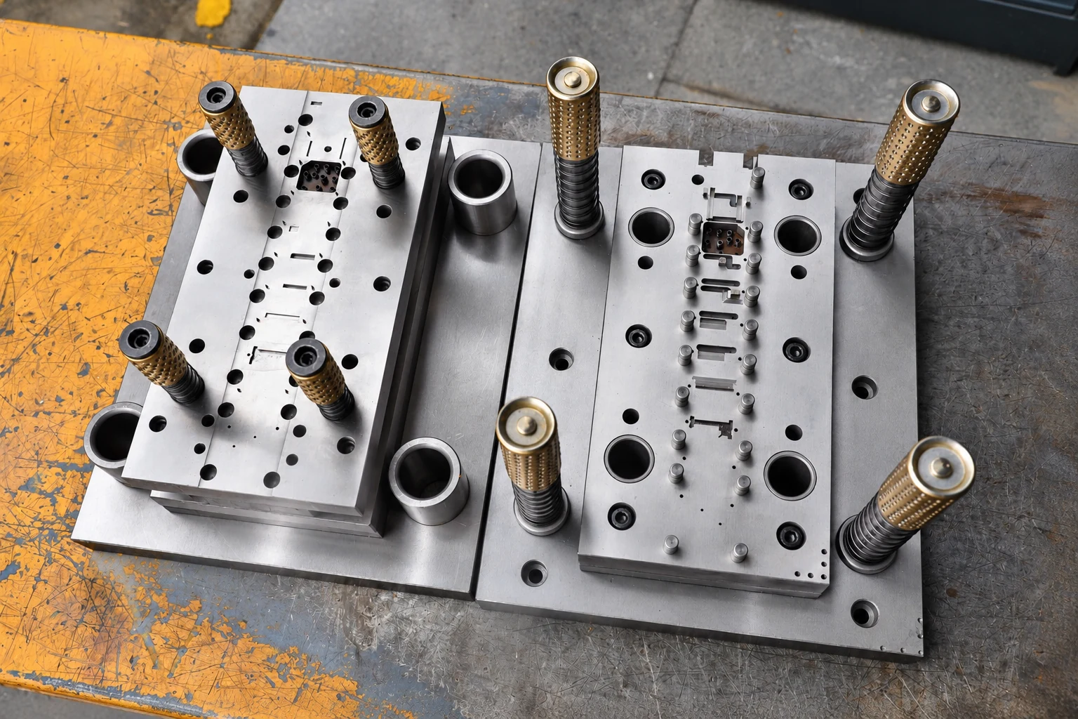
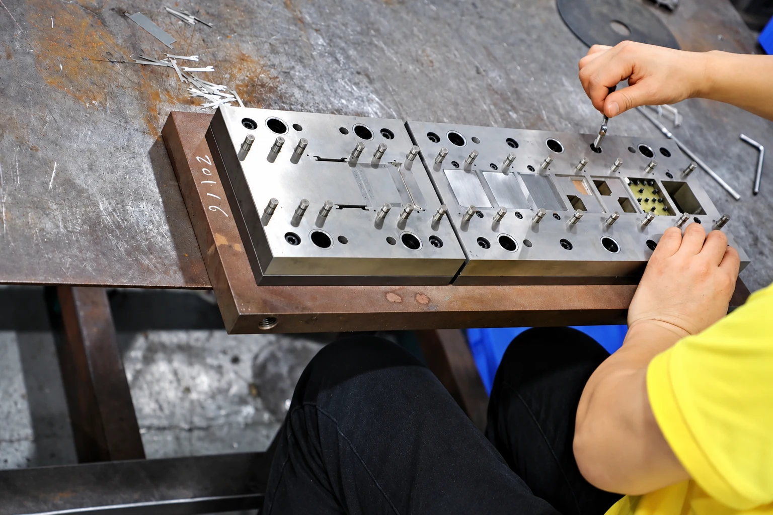
Paid samples include a full dimensional inspection report. Define drawing datums, acceptance criteria and corresponding mating parts so measurement and installed-fit checks can each answer the correct question. Confirm the charges, responsibilities and revision requirements for design changes, tooling work and later production stages within the project scope.
Paid samples and project planning
Samples are chargeable. Reference planning: standard samples 3–5 days; expedited sampling 48 hours; tooling and sample production 7–10 days. These are sample-stage arrangements, excluding mass-production delivery. The project plan is reviewed against the confirmed information, process and sample scope.
Related structures and project directions
Compare references through their coverage, installation and manufacturing tasks.
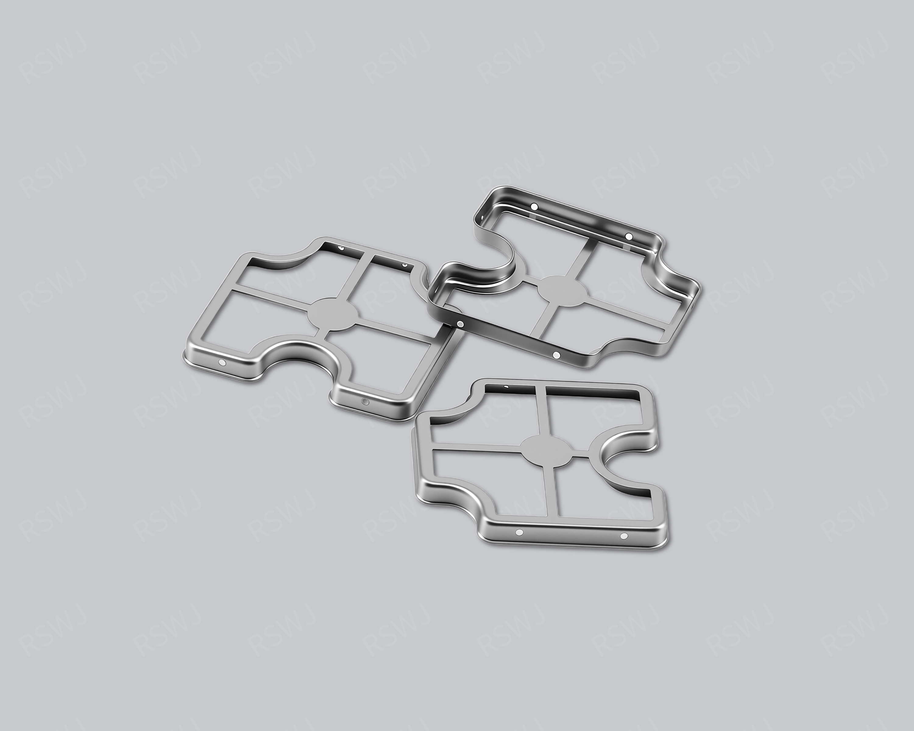
5G Circuit Shielding Can
A 5G shielding can is designed around a specified communication circuit region and its integration conditions.
Design & manufacturing details →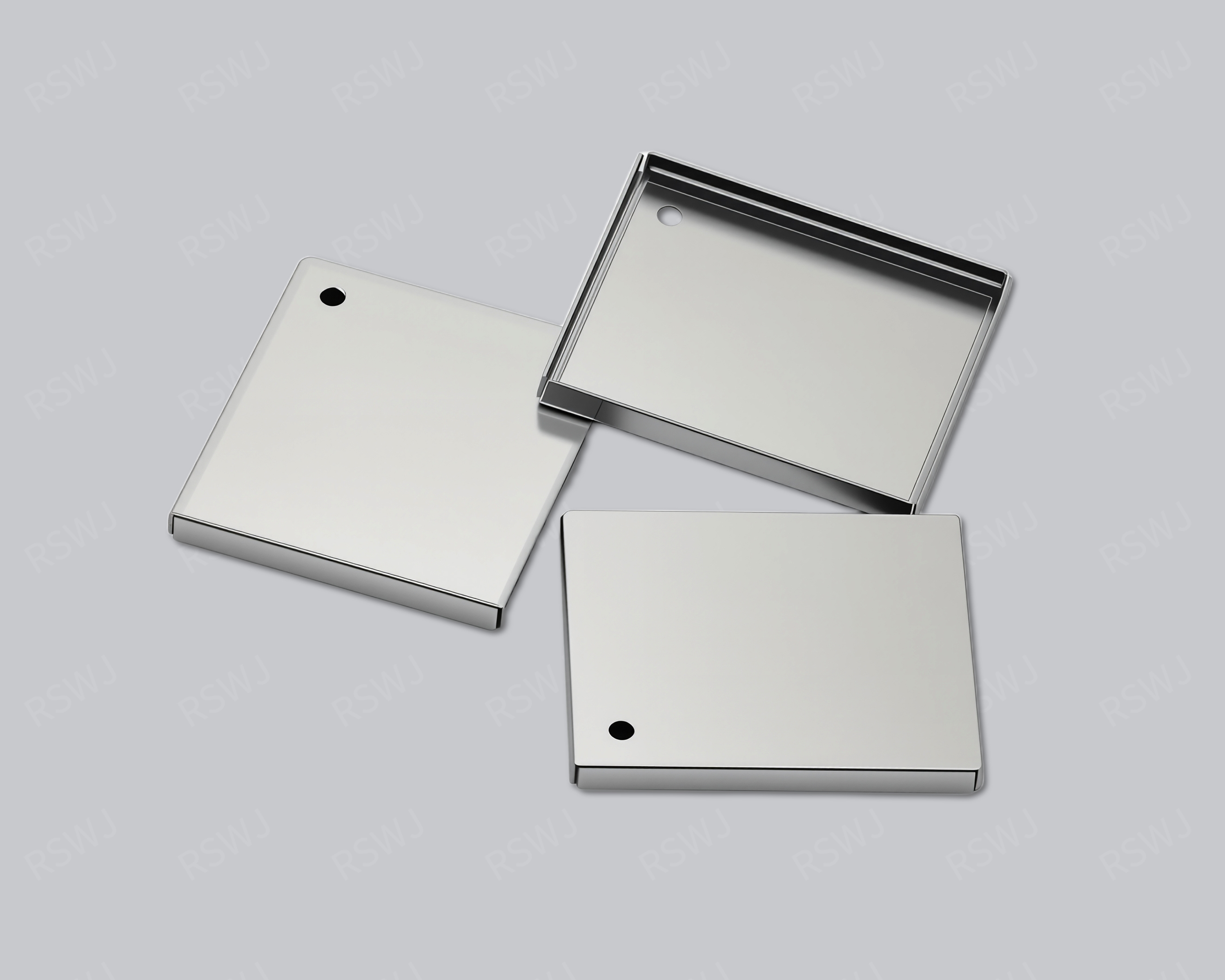
5G Module Shielding Can
A 5G shielding can is designed around a specified communication circuit region and its integration conditions.
Design & manufacturing details →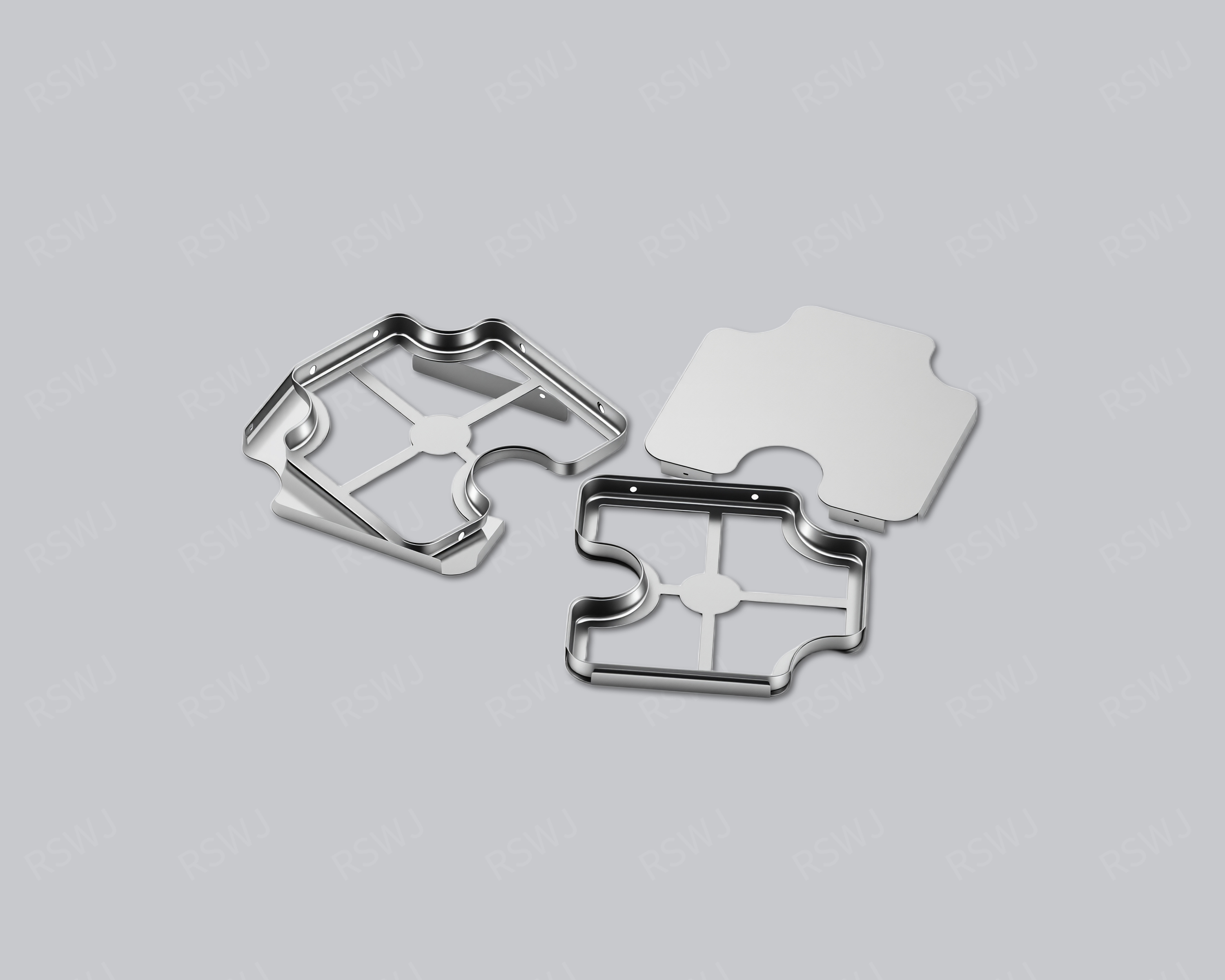
ADAS Module Shielding Can
An ADAS module shield is reviewed around the specific sensing, processing or communication circuit requiring coverage.
Design & manufacturing details →Discuss your BT Circuit Shielding Can project
Send the current drawing and mating conditions so we can review the structure, material, sample scope and required checks.
Send your project requirementsExplore electronic applications