
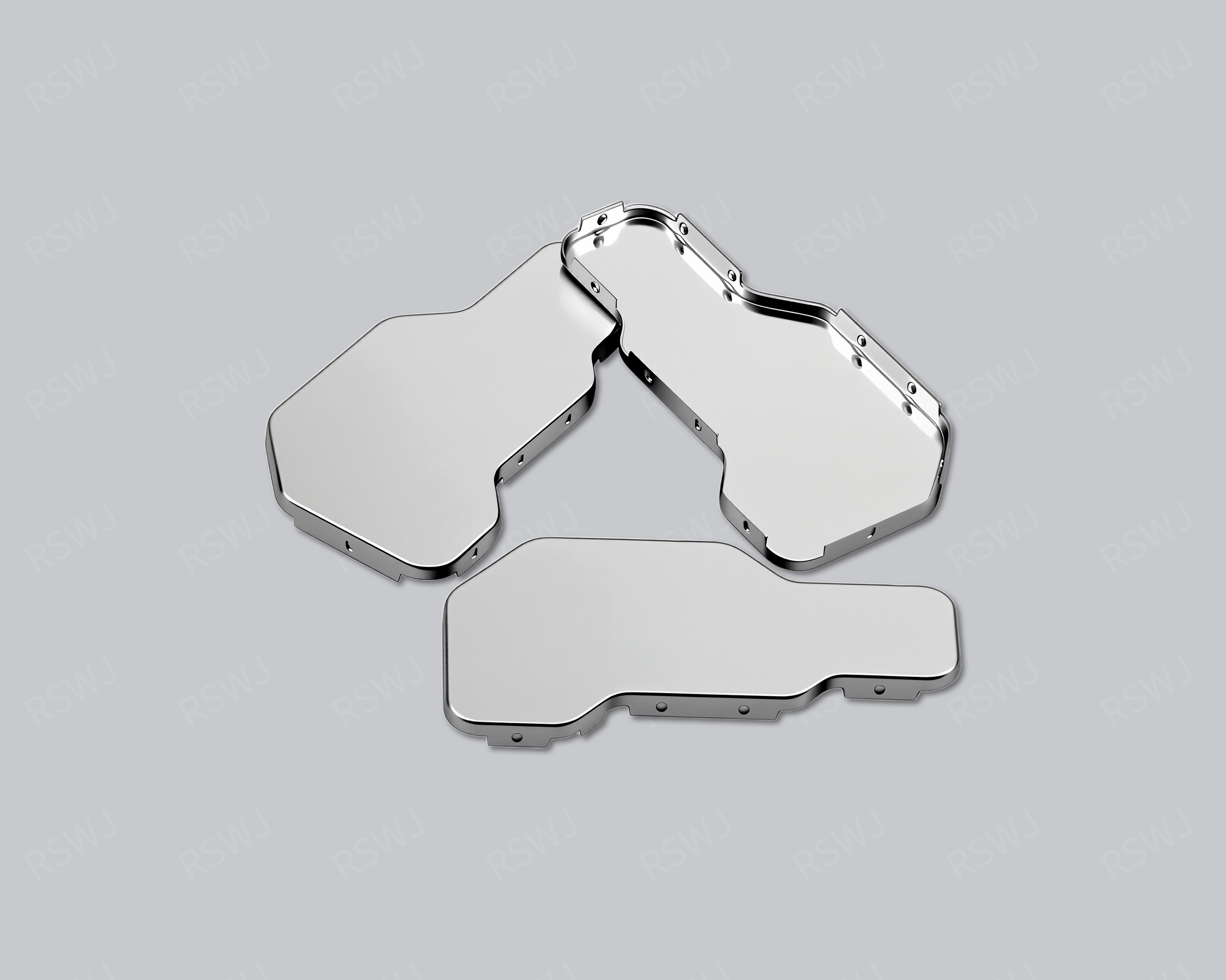
Reference photograph. Material, dimensions and mating requirements are defined in the agreed project drawings.
Connect the can landing to PCB references
A PCB shielding can coordinates metal coverage with board reference connections, keepouts and component placement.
| Design focus | PCB pads, reference regions, component keepouts and installed posture |
|---|---|
| Project task | Connect the can landing to PCB references |
| Custom inputs | Current drawings, mating parts, material and final surface, quantity and acceptance requirements. |
Connect the can landing to PCB references
The shielding boundary includes the can and the circuit-board arrangement. Wall placement, cross-boundary traces and attachment regions need to be understood together rather than treated as an independent metal outline.
The board layout should identify the can attachment perimeter and the reference regions associated with it. Mark signals, supply connections and connectors approaching or crossing that perimeter. This allows wall placement and opening requirements to be reviewed with the board design instead of after the metal outline is frozen. Define the inspection datum from the installed PCB relationship, and use the same revision when checking the bare can, its attachment and final component clearance.
Engineering considerations for this project
Translate the land pattern into a manufacturable attachment edge
A board land pattern and a metal attachment edge describe opposite sides of the same installed interface. Provide a view that relates them through a common locating reference, including any mounting feature used to establish orientation. A drawing that dimensions every metal feature from an external corner may still need a transformation to explain how those features meet the PCB. Resolve that relationship in the assembly definition before selecting the dimensions used for acceptance. It gives the engineer a way to review a local attachment change without repeatedly shifting the whole shield outline to obtain a visual match.
Separate the regions intended for attachment from nearby conductors and component keep-outs. Show whether a local interruption exists for a connector, signal route or another necessary board feature. The purpose of that interruption helps the team discuss its location and the surrounding formed geometry. Where an existing PCB constrains the pattern, state that constraint explicitly and identify which metal features remain open to review. This prevents a manufacturing suggestion intended to improve forming from moving an interface that the current board cannot accommodate. The approved metal and board views should ultimately describe the same attachment locations. Define any position that must stay aligned with existing PCB lands during future revisions.
Coordinate the lower edge with the populated board
The populated PCB gives the attachment discussion its usable space. Include component body envelopes and relevant height information near the shield walls, with the board revision used to approve them. The clearance needed to place the can may differ from its clearance after seating, especially around tall neighboring parts. A local notch may be helpful for installation yet unnecessary in the final position; either way, its reason should appear in the brief. Review a proposed edge or wall revision with the actual placement direction so that a nominal fit does not conceal an obstructed operation.
Where the can shares space with connector or cable operations, include the disconnected and connected conditions required by the assembly sequence. The connector body alone does not show the motion of a latch, tool or cable during that work. If an operation must happen before shielding is installed, identify it as a prerequisite rather than enlarging an opening without context. These choices affect both the outline and the inspection access available later. They are useful to review while the PCB relationship is being defined because a late access problem can require a different attachment or closure concept.
Use board changes to define the recheck scope
A PCB revision may preserve its outer dimensions while changing the shield relationship. Compare the attachment locations, nearby component envelopes and crossing interfaces between revisions. Mark the affected wall or opening on the metal drawing and identify any unchanged datum that still provides the locating basis. The next sample check can then concentrate on a known change while retaining the accepted relationships elsewhere. This is more informative than requesting a general new fit check without showing which populated feature moved or why the former assembly record may no longer represent the revised board.
During sample fitting, record the board revision and attachment condition used to establish the installed position. Locate a concern through that relationship before deciding whether to revise the formed edge, a board feature or the placement operation. If a corresponding lid or housing is involved, identify its version and the stage at which the issue appears. A successful check on one board configuration should remain tied to that configuration. These records provide a usable acceptance basis for the PCB shielding can and make subsequent compatibility discussions specific enough for engineering and procurement to act on.
A closer review of this project task
A PCB shield drawing should relate the metal attachment features to the board land pattern and the intended circuit reference connections. Show the locating basis used by both the PCB layout and the formed part. Identify signals, connectors or supply paths that approach or cross the planned coverage edge, and mark component keep-outs that restrict wall placement. The board outline alone does not describe these relationships. Including them in the brief allows a proposed wall or opening change to be assessed against the actual connection and clearance requirements before the metal drawing is frozen.
Use the corresponding board revision for the sample installation check. Inspect the attachment relationship and component space, then locate any mismatch against the PCB and part references. If a layout change moves a land, connector or keep-out, identify the affected metal feature rather than accepting compatibility because the board dimensions remain unchanged. Keep the joining or mounting condition with the observation, especially where the final installed position differs from the bare-part measurement. This produces a practical approval basis for the can-to-PCB relationship and a clearer change record for later board revisions.
Boundary, clearance and mating design
Use the board layout to locate pads, reference regions, component heights and interface exits. A consistent assembly datum links board mounting and formed-part inspection.
Translate the application into an actual circuit region. Mark the devices, interfaces and surrounding functions involved in the project concern. The equipment name can help organize discussion, but it does not provide hidden dimensions, compatibility or operating performance. Identify what must remain outside the metal boundary, such as a functional antenna, optical region or connection operation. The perimeter then follows a defined electronic and mechanical task rather than an arbitrary rectangle around the board.
Material and final surface definition
Select the material and final surface through forming, attachment, contact and the customer environment. The application label does not determine an alloy or coating for the reference. Specify grade, condition and thickness where required, with the final treatment separate. A working cover edge and a board joining region may need different checks. If a material alternative is evaluated, keep its changed conditions clear instead of treating it as an interchangeable color or marketing designation.
Forming and the installation sequence
Define joining or mounting conditions and the order of board inspection. Check the part after attachment so the installed posture and final cover interfaces are visible.
Use the real mounting references and component envelopes to establish fit. Review the path used to place the shield, connect interfaces and fit the surrounding housing. The final position can clear a connector while the required insertion motion remains blocked. Mark intentional contacts separately from required gaps. When another part loads the roof, check the installed state rather than using an unloaded cover height as the full clearance decision.
Choose datums from the board-mounted assembly
Compare outlines and closure options with the PCB landing, keepouts and component heights. A datum convenient on the loose can should also be meaningful for installation. Define the points that locate the body and the regions that need contact, then identify signals and connectors crossing the wall. If the board changes, review those relationships rather than accepting an unchanged can because its outside length and width still match the board outline.
Part inspection and application evaluation
Distinguish bare-part acceptance from board-mounted fit and system evaluation. Keep the PCB revision, attachment condition and operating arrangement tied to each sample record.
A drawing package for this custom part
| Input | What makes it usable |
|---|---|
| Coverage & interfaces | PCB pads, reference regions, component keepouts and installed posture. Mark their relationship with the actual circuit or mating layout; identify fixed references and permitted changes. |
| Final part & datums | A dimensioned finished-part drawing and available 3D information. Identify functional dimensions, the installed condition and the measurement references used to accept them. |
| Material & surface | The specified grade, condition, thickness and final treatment. Show contact, joining and insulated regions separately; identify any alternative that needs evaluation. |
| Assembly & acceptance | Corresponding mating revisions and the installation or access sequence. Distinguish part inspection, matched fit and customer system checks with their agreed conditions. |
Questions for this design review
How do you locate an issue that appears only after attachment?
Record bare-part measurements, then inspect the part on the corresponding PCB with the intended mounting operation. Identify where posture or clearance first differs. If a later lid is involved, check its mating interface after attachment. These stages distinguish a forming concern from a board or joining relationship. Keep the PCB and can revisions with the observations so the next change has a clearly defined target.
Which drawings support the review of PCB Shielding Can?
Use the current layout and mating assembly to identify PCB pads, reference regions, component keepouts and installed posture. Mark the relationship that is already fixed and the specific feature being considered for change. A drawing of the cover alone may omit the condition that gives the reference its engineering purpose. Include the corresponding board or base and the intended operation so the proposed revision can be evaluated against a defined task rather than a similar-looking external shape.
In-House Tooling & Formed-Part Quality
Tooling development and forming quality
The manufacturing review for PCB Shielding Can connects how critical features are formed, how they are inspected and how they meet the mating assembly. Ruishuo links in-house die design and CAD/CAM simulation with stamping. Die-making output of more than 100 sets per month is a factory capability; the tool concept is reviewed for the actual project.
Board zoning and attachment-edge location
Board-level shielding tooling converts the circuit layout into a manufacturable and measurable boundary. Relate attachment edges, interface openings and component clearance to the same PCB revision. Board-layout changes may affect tool-controlled locating and keep-out features.
- Board-related datums
- Define attachment and opening dimensions from explicit PCB-compatible references, with the coverage areas shown on the corresponding layout.
- Mechanical and circuit validation
- Check the dimensional report first, then assess coverage, contact and interface clearance with the actual PCB. System validation uses the agreed operating configuration.
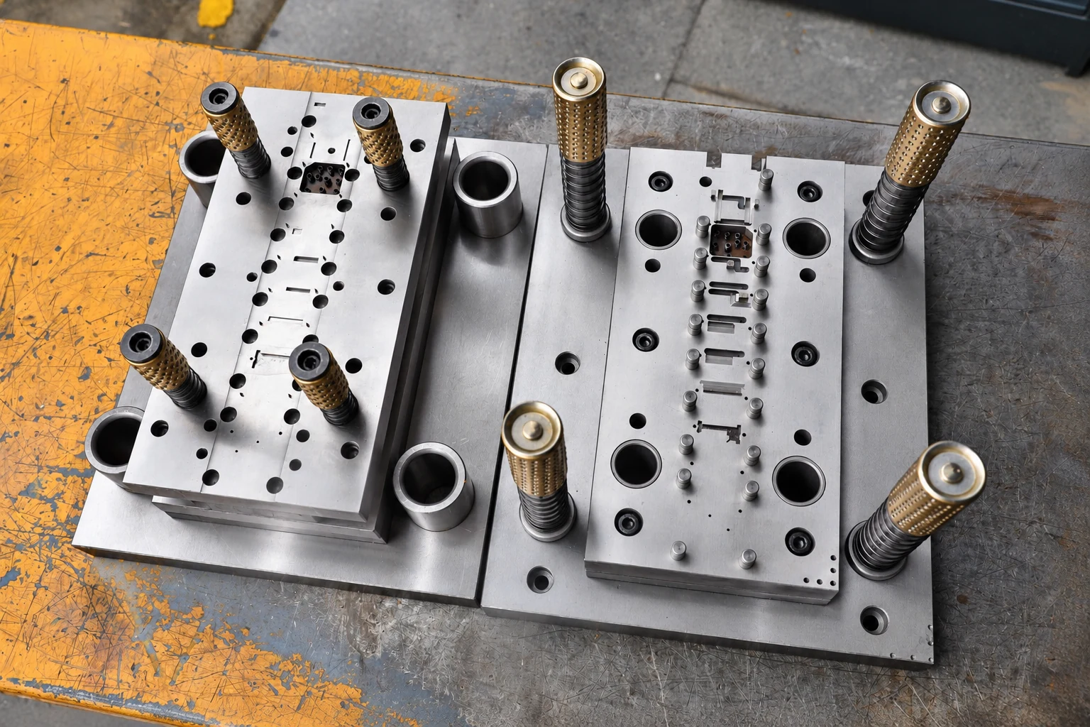
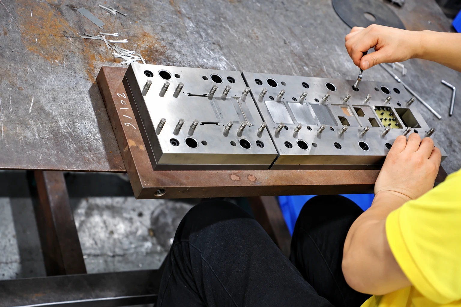
Paid samples include a full dimensional inspection report. Define drawing datums, acceptance criteria and corresponding mating parts so measurement and installed-fit checks can each answer the correct question. Confirm the charges, responsibilities and revision requirements for design changes, tooling work and later production stages within the project scope.
Paid samples and project planning
Samples are chargeable. Reference planning: standard samples 3–5 days; expedited sampling 48 hours; tooling and sample production 7–10 days. These are sample-stage arrangements, excluding mass-production delivery. The project plan is reviewed against the confirmed information, process and sample scope.
Related structures and project directions
Compare references through their coverage, installation and manufacturing tasks.
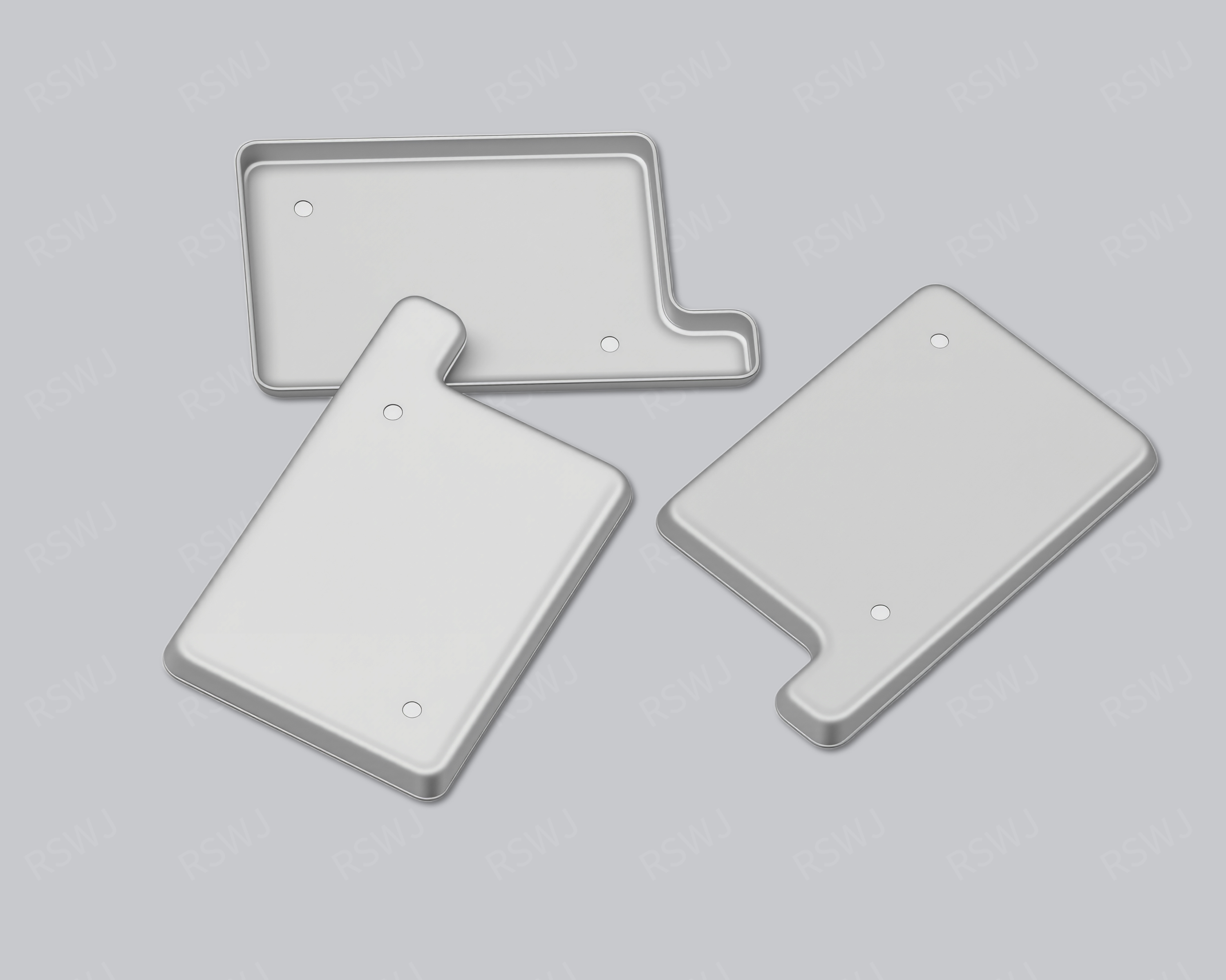
Mainboard Circuit Shielding Can
A PCB shielding can coordinates metal coverage with board reference connections, keepouts and component placement.
Design & manufacturing details →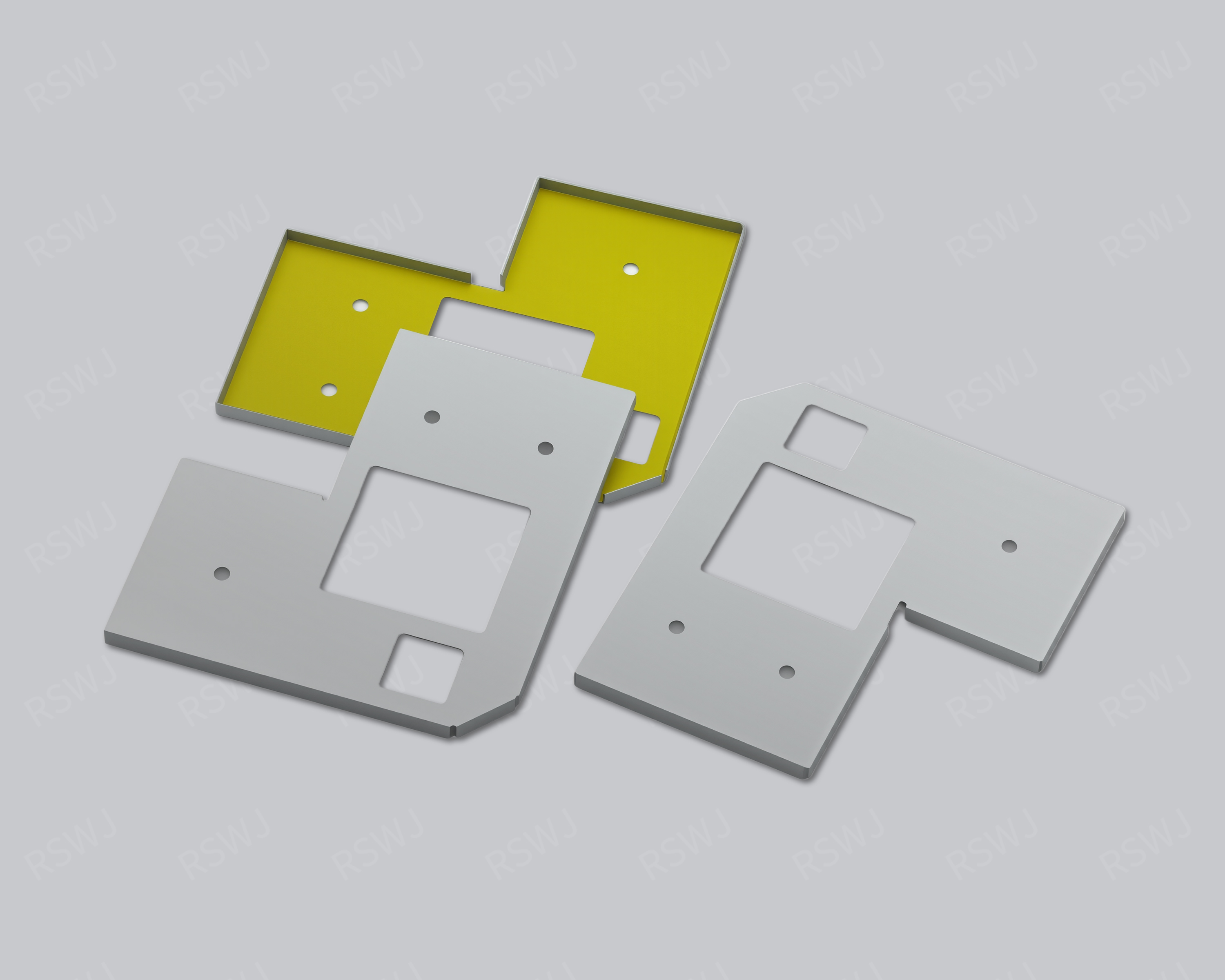
Mainboard Shielding Can
A PCB shielding can coordinates metal coverage with board reference connections, keepouts and component placement.
Design & manufacturing details →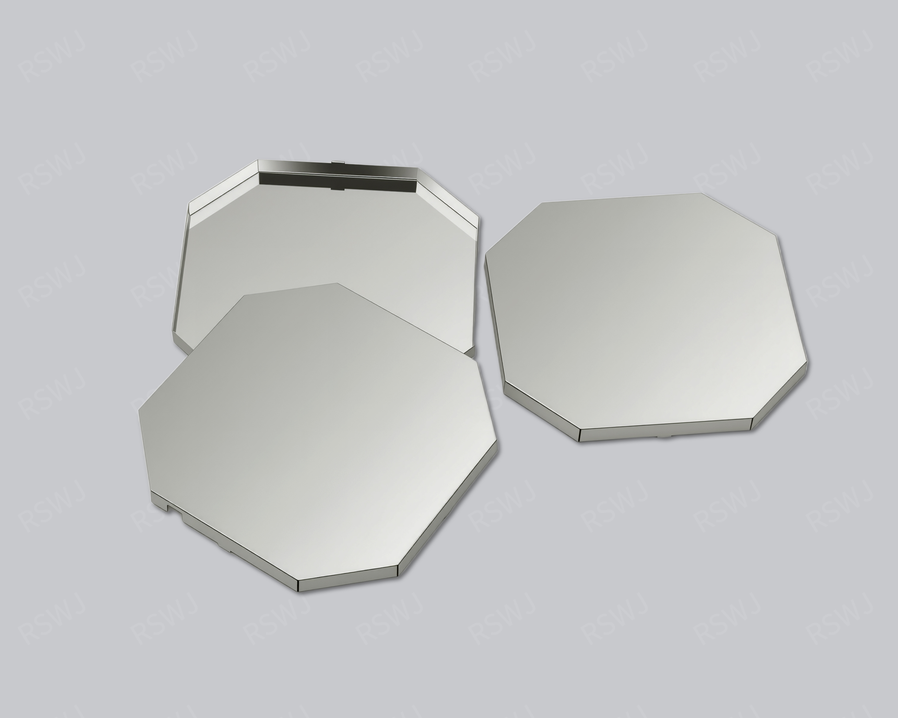
Custom Mainboard Shielding Can
A PCB shielding can coordinates metal coverage with board reference connections, keepouts and component placement.
Design & manufacturing details →Discuss your PCB Shielding Can project
Send the current drawing and mating conditions so we can review the structure, material, sample scope and required checks.
Send your project requirementsExplore electronic applications